In resent days, the research team led by Prof. Ni Zhenhua and Prof. Wang Jinlan from the School of Physics, Southeast University utilized the defect engineering to upgrade the properties of two-dimensional photoconductor. Their research achievement titled “Defect Engineering for Modulating the Trap States in Two-dimensional Photoconductor” has been published on important periodical in the field of material: Advanced Materials.
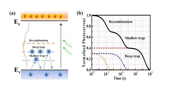
The photoconductor, as a kind of device that transfers light to electrical signal, has been deemed as one of the key technologies that can exert effect on our daily life, science & technology, and national defence, etc. such as video imaging, photo-communication, biomedical imaging, sensing, night viewing, security and military reconnaissance, etc.. Since the defect state of the semiconductor material, as the trapping centre, can prolong the life of carriers effectively, the introduction of photoconduction gains can increase the sensitivity of photoconductor to a large extent; however, the trapping centre, especiallywith the introduction of deep trap, can increase the device’s response time sharply mainly because it takes additional time for the carriers to get rid of the trap of defect state. Moreover, such time also depends on the level of defect state (Fig. 1). It has been always the difficulty confronted in this field to achieve rapid response while the device’s high sensitivity can be guaranteed as well by means of the control of defect state and trapping centre. In contrast to traditional semiconductor materials, the energy band structure of two-dimensional materials can modulate in a more effective way though the surface and defect engineering; besides, it has also provided ideal research object to find solution to the said difficulty.
Schematic diagram of the process of stimulation, recombination and trapping of photon-generated carriers in n-type semiconductor (including the trap state at deep and shallow energy levels) (a), and the response time of corresponding device engaged in these processes (b)
The two-dimensional materials include diversified defects and can exert significant influences on their electrical, optical, magnetic and mechanical properties, etc.. In early 2018, Prof. Ni Zhenhua cooperated with the research team led by Prof. Chen Wei. They published an overview paper titled “Two-dimensional transition metal dichalcogenides: interface and defect engineering” on Chemical Society Reviews, which analysed the impact of defect and interface states on the electrical and photoelectric properties of two-dimensional chalcogenides in detail and how to modulate the properties of two-dimensional electronic/photo-electronic devices by means of the defect and interface engineering.
In this work, the research team led by Prof. Ni Zhenhua and Prof. Wang Jinlan, taking ReS2 as a study case, initiated from the experiment andcomputational simulation respectively, then proposed utilizing the defect engineering to control the trap state of carriers in the two-dimensional photoconductor. The research result indicated that the oxygen atom in the protoporphyrin (H2PP) molecule can bind to the surrounding rhenium atom at the sulphur vacancy of ReS2 and function in regulating the band structure and the defect energy levels. Compared with the photoelectric response dominated by the deep trap in the original sample, the photo-response of the modified device would be dominated by the shallow trap and the recombination centre, meanwhile, the response speed has been increased by three to four orders (Fig. 2). In addition, since there’s a strong charge transfer between H2PP molecules and ReS2, the surplus electrons in ReS2 can be extracted, thereby greatly reducing the dark current and noise of the device while enabling the light detection rate of the modified device to reach 1.89x10^13 Jones. This work has provided a research idea about how to control the trap state of photo-induced carriers in semiconductors through the defect engineering, which would be conducive to achieve two key indicators of high sensitivity and fast response in photo-detectors simultaneously.
Response time curve of ReS2 photo-detector before/after H2PP molecular modification
The first authors of this paper are Dr. Jiang Jie and Dr. Ling Chongyi from the School of Physics, Southeast University; Prof. Ni Zhenhua and Prof. Wang Jinlan are the joint corresponding authors. This project has been sponsored by National Key R&D Program and Natural Science Foundation of China (NSFC), etc..
Thesis links:
Advanced MaterialsDOI:10.1002/adma.201804332 (2018): https://onlinelibrary.wiley.com/doi/abs/10.1002/adma.201804332
Chemical Society Reviews 47, 3100 (2018): http://pubs.rsc.org/en/Content/ArticleLanding/2018/CS/C8CS00024G#!divAbstract